- 您现在的位置:买卖IC网 > Sheet目录1214 > EVAL-ADE7754EBZ (Analog Devices Inc)BOARD EVALAUTION FOR ADE7754
�� ����
����
����ADE7754�
�TERMINOLOGY�
�Measurement� Error�
�The� error� associated� with� the� energy� measurement� made� by� the�
�ADE7754� is� defined� by� the� formula�
�Percentage� Error� =�
�AV� DD�
�5V�
�4V�
�?�
�?�
�� 100%� ?�
�?� Energy Registered by ADE� 7754� ?� True Energy�
�True� Energy�
�?�
�?�
�0V�
�TIME�
�Phase� Error� Between� Channels�
�The� HPF� (high-pass� filter)� in� the� current� channel� has� a� phase�
�POWER-ON�
�ACTIVE�
�INACTIVE�
�lead� response.� To� offset� this� phase� response� and� equalize� the�
�phase� response� between� channels,� a� phase� correction� network� is�
�placed� in� the� current� channel.� The� phase� correction� network�
�ensures� a� phase� match� between� the� current� channels� and� voltage�
�channels� to� within� ±� 0.1� °� over� a� range� of� 45� Hz� to� 65� Hz� and�
�±� 0.2� °� over� a� range� of� 40� Hz� to� 1� kHz.� This� phase� mismatch�
�between� the� voltage� and� the� current� channels� can� be� reduced�
�further� with� the� phase� calibration� register� in� each� phase.�
�Power� Supply� Rejection�
�This� quantifies� the� ADE7754� measurement� error� as� a� percentage�
�of� reading� when� power� supplies� are� varied.� For� the� ac� PSR� mea-�
�surement,� a� reading� at� nominal� supplies� (5� V)� is� taken.� A� second�
�reading� is� obtained� using� the� same� input� signal� levels� when� an� ac�
�(175� mV� rms/100� Hz)� signal� is� introduced� onto� the� supplies.� Any�
�error� introduced� by� this� ac� signal� is� expressed� as� a� percentage� of�
�reading.� See� the� Measurement� Error� definition� above.�
�For� the� dc� PSR� measurement,� a� reading� at� nominal� supplies�
�(5� V)� is� taken.� A� second� reading� is� obtained� using� the� same�
�input� signal� levels� when� the� power� supplies� are� varied� ±� 5%.� Any�
�error� introduced� is� again� expressed� as� a� percentage� of� reading.�
�ADC� Offset� Error�
�This� refers� to� the� dc� offset� associated� with� the� analog� inputs� to�
�the� ADCs.� It� means� that� with� the� analog� inputs� connected� to�
�AGND,� the� ADCs� still� see� a� dc� analog� input� signal.� The� magni-�
�tude� of� the� offset� depends� on� the� gain� and� input� range� selection�
�(see� the� TPCs).� However,� when� HPFs� are� switched� on,� the�
�offset� is� removed� from� the� current� channels� and� the� power�
�calculation� is� unaffected� by� this� offset.�
�Gain� Error�
�The� gain� error� in� the� ADE7754� ADCs� is� defined� as� the� differ-�
�ence� between� the� measured� ADC� output� code� (minus� the�
�offset)� and� the� ideal� output� code.� See� the� Current� Channel�
�ADC� and� the� Voltage� Channel� ADC� sections.� The� difference� is�
�expressed� as� a� percentage� of� the� ideal� code.�
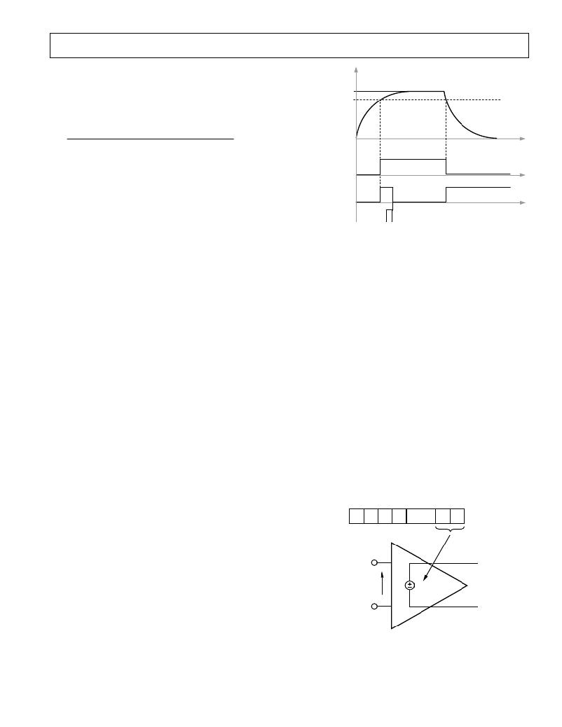
�RESET� FLAG� IN�
�THE� INTERRUPT�
�STATUS� REGISTER�
�READ� RSTATUS�
�REGISTER�
�Figure� 4.� On-Chip� Power� Supply� Monitoring�
�The� RESET� bit� in� the� interrupt� status� register� is� set� to� Logic� 1�
�when� AV� DD� drops� below� 4� V� ±� 5%.� The� RESET� flag� is� always�
�masked� by� the� interrupt� enable� register� and� cannot� cause� the�
�IRQ� pin� to� go� low.� The� power� supply� and� decoupling� for� the�
�part� should� ensure� that� the� ripple� at� AV� DD� does� not� exceed� 5� V�
�±� 5%� as� specified� for� normal� operation.�
�ANALOG� INPUTS�
�The� ADE7754� has� six� analog� inputs,� divisible� into� two� chan-�
�nels:� current� and� voltage.� The� current� channel� consists� of� three�
�pairs� of� fully� differential� voltage� inputs:� I� AP� ,� I� AN� ;� I� BP� ,� I� BN� ;� and�
�I� CP� ,� I� CN� .� The� fully� differential� voltage� input� pairs� have� a� maxi-�
�mum� differential� voltage� of� ±� 0.5� V.� The� voltage� channel� has�
�three� single-ended� voltage� inputs:� V� AP� ,� V� BP� ,� and� V� CP� .� These�
�single-ended� voltage� inputs� have� a� maximum� input� voltage� of�
�±� 0.5� V� with� respect� to� V� N� .� Both� the� current� channel� and� the�
�voltage� channel� have� a� PGA� (programmable� gain� amplifier)� with�
�possible� gain� selections� of� 1,� 2,� or� 4.� The� same� gain� is� applied� to�
�all� the� inputs� of� each� channel.�
�The� gain� selections� are� made� by� writing� to� the� gain� register.� Bits� 0�
�and� 1� select� the� gain� for� the� PGA� in� the� fully� differential� current�
�channel.� The� gain� selection� for� the� PGA� in� the� single-ended� volt-�
�age� channel� is� made� via� Bits� 5� and� 6.� Figure� 5� shows� how� a� gain�
�selection� for� the� current� channel� is� made� using� the� gain� register.�
�GAIN[7:0]�
�Gain� Error� Match�
�Gain� error� match� is� defined� as� the� gain� error� (minus� the� offset)�
�obtained� when� switching� between� a� gain� of� 1,� 2,� or� 4.� It� is�
�expressed� as� a� percentage� of� the� output� ADC� code� obtained�
�I� AP� ,� I� BP� ,� I� CP�
�GAIN� (k)�
�SELECTION�
�under� a� gain� of� 1.�
�V� IN�
�k�
�V� IN�
�POWER� SUPPLY� MONITOR�
�The� ADE7754� contains� an� on-chip� power� supply� monitor.� The�
�analog� supply� (AV� DD� )� is� continuously� monitored� by� the� ADE7754.�
�If� the� supply� is� less� than� 4� V� ±� 5%,� the� ADE7754� goes� into� an�
�inactive� state� (i.e.,� no� energy� is� accumulated� when� the� supply�
�voltage� is� below� 4� V).� This� is� useful� to� ensure� correct� device�
�operation� at� power-up� and� during� power-down.� The� power� sup-�
�ply� monitor� has� built-in� hysteresis� and� filtering,� providing� a� high�
�degree� of� immunity� to� false� triggering� due� to� noisy� supplies.�
�REV.� 0�
�–9� –�
�I� AN� ,� I� BN� ,� I� CN�
�Figure� 5.� PGA� in� Current� Channel�
�发布紧急采购,3分钟左右您将得到回复。
相关PDF资料
EVAL-ADE7755ZEB
BOARD EVALUATION FOR AD7755
EVAL-ADE7758ZEB
BOARD EVAL FOR AD7758
EVAL-ADE7759EBZ
BOARD EVALUATION FOR ADE7759
EVAL-ADE7762EBZ
BOARD EVALUATION FOR ADE7762
EVAL-ADE7763ZEB
BOARD EVALUATION FOR ADE7763
EVAL-ADE7816EBZ
BOARD EVALUATION FOR ADE7816
EVAL-ADE7878EBZ
BOARD EVAL FOR ADE7878
EVAL-ADE7880EBZ
BOARD EVAL FOR ADE7880
相关代理商/技术参数
EVAL-ADE7755EB
制造商:Analog Devices 功能描述:EVAL BOARD ENERGY METERINGW/PULSE OUTPUT - Bulk
EVAL-ADE7755EBZ
制造商:AD 制造商全称:Analog Devices 功能描述:Energy Metering IC with Pulse Output
EVAL-ADE7755EBZ1
制造商:AD 制造商全称:Analog Devices 功能描述:Energy Metering IC with Pulse Output
EVAL-ADE7755ZEB
功能描述:BOARD EVALUATION FOR AD7755 RoHS:是 类别:编程器,开发系统 >> 评估演示板和套件 系列:- 标准包装:1 系列:- 主要目的:电信,线路接口单元(LIU) 嵌入式:- 已用 IC / 零件:IDT82V2081 主要属性:T1/J1/E1 LIU 次要属性:- 已供物品:板,电源,线缆,CD 其它名称:82EBV2081
EVAL-ADE7756EB
制造商:Analog Devices 功能描述:EVAL BD DOCUMENTATION ADE7756 ENERGY METERING IC - Bulk 制造商:Rochester Electronics LLC 功能描述:
EVAL-ADE7757AEBZ
制造商:Analog Devices 功能描述:EVALUATION BOARDS - Bulk
EVAL-ADE7757EB
制造商:Analog Devices 功能描述:EVAL BOARD ENERGY METERINGW/PULSE OUTPUT - Bulk
EVAL-ADE7758ZEB
功能描述:BOARD EVAL FOR AD7758 RoHS:是 类别:编程器,开发系统 >> 评估演示板和套件 系列:* 标准包装:1 系列:PSoC® 主要目的:电源管理,热管理 嵌入式:- 已用 IC / 零件:- 主要属性:- 次要属性:- 已供物品:板,CD,电源